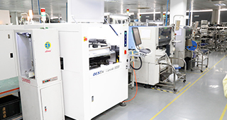
SMT often has basic knowledge of electronic components
1. Classification of common electronic components:
(1), resistance class (Res): electronic symbol R
Chip resistor, color ring resistance,
Varistor, temperature sensitive resistor
(2), Capacitor (Cap): Electronics Symbol C
Chip capacitor, safety capacitor, electrolytic capacitor
Magnetic chip capacitor, polyester capacitor, tantalum capacitor
(3), inductance class (IND): electronic symbol L
Chip laminated inductor, chip winding inductor
Color ring inductor, wirewound inductor
(4), Diode (DIO): Electronic Symbol D
SMD diode, silicon diode,
Helium diode, light emitting diode
(5), Transistor (TRA): Electronic Symbol Q§T
(6), switch (KEY): electronic symbol SW
Dial switch, push button switch
(7), integrated circuit (IC): electronic symbol U
QFP, PLCC, SOP, BGA
(8), crystal oscillator (CRYSTAL): electronic symbol Y
(9), socket (JACK): Electronic symbol J
(10), optocoupler (OPTO)
(11), transformer
(12), FUSE (insurance tube)
2. Common electronic component units and conversion:
(1), resistance:
Basic unit: ohm symbol: Ω
Commonly used units: thousand ohms symbol: KΩ
Megaohm symbol: MΩ
Conversion relationship: 1MΩ=1000KΩ=1000000Ω
(2), capacitor:
Basic unit: Farah symbol: F
Commonly used unit: millifarad symbol: mF
Microfarad symbol: μF
Nafa symbol: nF
Pifa symbol: pF
Conversion relationship:
1F=103mF=106μF=109nF=1012pF
(3), inductance:
Basic unit: Henry symbol: H
Commonly used units: millihen symbol: mH
Micro-Heng symbol: uH
Nachen symbol: nH
Conversion relationship:
1H=103mH=106μH=109nH
3: Common electronic component error and pressure resistance representation
(1), error letter recognition method:
CDJKMZ
±0.25pF ±0.5pF ±5% ±10% ±20% +80% -20%
(2), pressure letter recognition method:
ABC
25V 50V 100V
SMD component specification
1: usually combined with the length and width of the patch component, indicating the patch component
A representation of the size, usually in inches (Inch) (1Inch = 2.54cm)
2: The specifications of common patch components are as follows:
A: 0402 indicates the component: length 0.04Inch width 0.02Inch
B: 0603 indicates the component: 0.06Inch length 0.03Inch
C: 0805 indicates the component: length 0.08Inch width 0.05Inch
D: 1206 indicates the component: length 0.12Inch width 0.06Inch
E: 1210 indicates the component: length 0.12Inch width 0.1Inch
Standard for judging the correctness of smt materials
1: The code on the material tray must correspond to the code on the customer list.
2: The model number of the material must correspond to the model number on the customer list.
3: The specifications of the materials should meet the requirements on the customer list.
4: The error of the material should meet the requirements on the customer list.
5: The silk screen on the physical object is consistent with the requirements on the customer list.
Must have valid file support from the customer.
6: There are special requirements to see the manufacturer's materials, the material manufacturers must meet the customer's requirements
Packaging of SMT materials
1: The packaging of the chip components usually uses a disk-shaped plastic disk.
2: Packaging of IC materials
IC components are usually packaged in TRAY disks. The TRAY specifications are usually expressed in terms of the number of (wideth and long) ICs that can be mounted on the TRAY disk.
Basic knowledge of pcba board
PCBA is the abbreviation of English Printed Circuit Board +Assembly, which means that the PCB blank board passes through the SMT upper part, and then passes through the whole process of DIP plug-in, referred to as PCBA. This is a commonly used method in the country, and the standard way of writing in Europe and America is PCB'A, which adds a slant point. This is called official idioms. When we communicate or promote with foreign customers, they often ask what PCBA means.
1, three-in-one board
The three-in-one board is a kind of lithium battery protection in order to save costs. Basic functions: over-discharge, over-charge, over-current, short-circuit, under-voltage because all functions are concentrated in the only IC control.
Therefore, in the case that this IC is broken, it may cause the PCBA board to lose control. In the process of charging, if the IC is broken, it is possible that the line is still connected, there is no IC overcharge protection, the power supply will still be charged when it is full, causing the battery to overcharge, the battery is hot, and even causing The battery burns or explodes.
2, with lithium battery protection board
PCBA with lithium protection is equivalent to double protection. Basic functions: over discharge, over charge, over current, short circuit, under voltage
That is, in the process of a large IC being broken, two small ICs can control the entire line. After the power is full, the line is disconnected for protection. Avoid hurting people and make bigger losses.
3, trim
The so-called trim is the waste discarded by the placement machine when it is mounted on the PCB, or the waste removed during the repair process, and recycled.
Such electronic materials are not unified, the accuracy of the electronic materials is not the same, and it may not meet the accuracy of the minimum requirements, and the abnormal operation of the PCBA may occur.
It will even cause leakage of the entire PCBA (that is, soldering a battery with electricity, put it overnight or put it for one day, the whole battery will be out of power)
4, ordinary single board
The input voltage is generally 5V, the current is 1A (±200MAH), the output voltage is generally 5V, and the current is 1A (±200MAH). The input of 1A is equivalent to 1 hour to charge the power supply to 1000MAH. The normal battery voltage is generally 3.7~4.2V. within
After the boost function of PCBA, the voltage of the power supply output is 5V, so that PCBA will heat up, and the micro heat generation of the power supply is normal.
5, the board is poor, medium, good
When the business quotes the customer, choose the medium and good price to send to the customer for comparison. If the price of the guest needs to be lower, then we also use the poor board to meet the price requirements of the customer.
The quality of the board is related to the price and price. Tell the guests that they have multiple choices.
Pcba board production process
PCBA's production process is mainly: purchase materials → solder paste printing → solder paste thickness gauge → placement machine placement → reflow soldering → AOI → DIP plug-in → wave soldering → post-weld cleaning → PCBA function test → finished product assembly → shipment
1, purchase materials
The PCBA processing plant purchases component materials, PCB boards, and stencils and fixtures according to the order placed by the customer.
2, solder paste printing
First, the solder paste just taken out of the cold room is thawed, stirred, and then accurately printed on the PCB pad by a solder paste printer.
3, solder paste thickness gauge
The printing effect of the solder paste is tested to check whether there is a case of tin, less tin, or missing.
4, placement machine placement
The placement machine accurately mounts the components onto the PCB pads by picking up components.
5, reflow soldering
The PCB with the components mounted is placed in the reflow soldering track, and the components are welded through the drying zone, the preheating zone, the welding zone and the cooling zone.
6, AOI testing
After the board is soldered, the AOI is used to test the soldering effect of the PCB and QA sampling is performed.
7, DIP plug-in processing
DIP production line workers simply process the insert and insert it into the corresponding position of the board.
8, wave soldering
The inserted board is placed in the wave soldering, and the PCBA board is soldered by spraying flux, preheating, wave soldering, cooling, and the like.
9, after welding cleaning
After the wave soldering, the PCBA board has many defects, and it is generally required to be repaired and cleaned. After the quality personnel check it, it can be transferred to the next process.
10, PCBA functional test
In the PCBA functional test, the PCBA board is generally subjected to ICT, FCT, aging test, and program firing to ensure the normal operation of the PCBA function and reduce the late repair rate.
11, finished product assembly
After the PCBA board has been tested for internal functions, the outer casing of the product is then assembled.
12, shipping
Finally, an OQC inspection of the finished product is required to confirm the correct shipment.
PCBA is a piece of PCB blank board processed through a series of processes, and finally processed into a user-friendly electronic product. In the process of production, a ring is buckled, and which link has quality problems, which have a great impact on the quality of the product.
